Heat distribution, power loss, structural effects: Simulation for power modules
René Fuger
16.04.2025
Using simulation in the development process to select the best design and material
Simulations are essential in the development of power modules in order to identify and optimize electrical, thermal and mechanical challenges at an early stage. Particularly important is the analysis of heat distribution, power loss and structural effects. We caught up with Gerald Weis, head of hardware development at PCB manufacturer AT & S, at the CADFEM Conference Salzburg, where he explained the trends and innovations that will shape the future of PCB technology.
Mr. Weis, your company produces power modules, among other things. How do simulations help you in this area?
Power modules must be able to handle a high power output. The components embedded in the circuit board generate high power losses – often 100 watts or more. This raises concerns, such as where problems may arise. Among other things, we want to know where the heat is trapped and what happens if the module is electrically insulated. We simulate these scenarios in the electrical, thermal and mechanical domains to ensure that the design meets the desired thermal and electrical requirements.
Our technology makes it possible to embed parts directly into the PCB during production, enabling more accurate analysis and better thermal management. The model then goes through several iterations. First, we integrate the simulation results, then optimize the design and check the effects on performance, both electrically and thermally. The model is then transferred to a hardware-in-the-loop simulation to validate the design. The goal for the future is to use artificial intelligence to further automate and optimize this process – a tremendous help for us and our customers.
Artificial intelligence, miniaturization, more computing power — we must keep investing in electro-thermal and mechanical simulation to meet new challenges. We want to continue to be a leader in PCB development by combining innovative technologies and advanced simulation techniques.
What role does simulation generally play in your development process?
These days, almost every component is simulated with a new part number, whether it is electrical, thermal or mechanical. We not only deal with printed circuit boards, but also with so-called IC substrates, which are used in the manufacture of integrated circuits. These integrated circuits are extremely complex. They can have up to 800,000 holes in a 30-by-30-millimetre area. Of course, this can cause structural-mechanical problems such as warping, buckling and twisting.
Simulation helps us to anticipate these problems. It also allows us to give feedback to the customer if, for example, a better performance could be achieved using a different design or material. Simulation is not only used at the design level, but also at the process level. We work together with the research department to further develop process simulations, particularly in the area of chemical and fluid solutions.

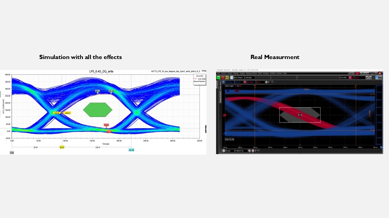
Software Based Validation | © Janagan Papperi Devarajulu Deenadayalan (AT & S Austria Technologie & Systemtechnik Aktiengesellschaft)
What are the biggest challenges in your field of work?
The biggest challenge is that customers often involve us too late. If we see during the simulation that something is not working optimally, it can lead to problems because we usually produce a single part of a full system. If one small thing needs to be changed, the other parts of the system must also be adapted.
Presentation CADFEM Conference Salzburg
Learn more about the topic ‘Electrothermal simulation of an embedded power module using ANSYS Maxwell & Icepak’ and download the presentation of Janagan Papperi Devarajulu Deenadayalan (AT & S Austria Technologie & Systemtechnik Aktiengesellschaft).
Download now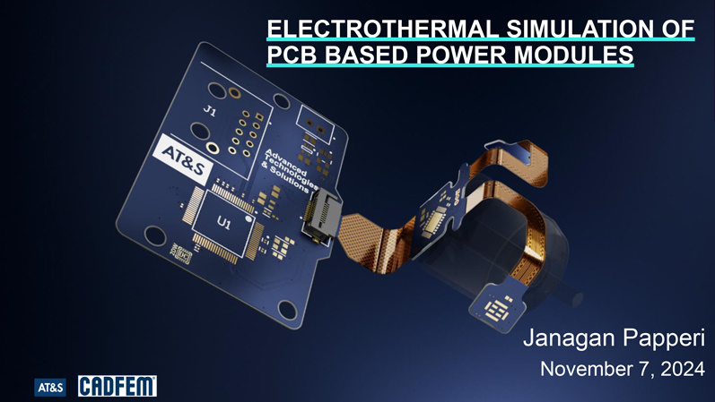
What role do electromagnetic simulations and other disciplines play in your development process?
At AT & S, we are initially focusing on electrical simulation, as this is crucial for the functionality of the components. The next step is electro-thermal simulation to check heat dissipation and thermal resistance. Particularly in power modules, it is important to efficiently extract heat to extend the life cycle of components. Thermal spreading, i.e. how well heat is transferred between the components, is a crucial factor here. This is followed by mechanical simulation to identify structural problems such as warpage or warping.
This process is iterative. We optimize the various simulations to achieve the best possible performance. However, it may also happen that a change in one area (e.g. mechanical simulation) affects the results in other areas (e.g. electrical or thermal simulation). In this case, it is important to evaluate the entire process and, if necessary, find the best compromise.
What future trends do you see for PCB technology and simulation?
There is no doubt that artificial intelligence is the biggest trend. Everything hinges on this. Among other things, artificial intelligence will allow chips to be produced in larger sizes. The IC substrate, for example, could go from 30 by 30 millimeters to 100 by 100 millimeters, or perhaps even more. However, miniaturization is also becoming increasingly important, meaning that things are also getting smaller. At the same time, there is a definite trend towards wanting more computing power.
This means we have to invest even more effort in electrothermal and mechanical simulation to meet new challenges. Our vision is to remain at the forefront of PCB development by combining innovative technologies and advanced simulation techniques.
Thank you very much for the interview, Mr. Weis.
Watch the full interview with Gerald Weis here.
Ansys HFSS
Industry standard for determining the radiation and transmission behavior of high-frequency electromagnetic fields.
