Accelerate Electronics Development: Cut Time-to-Market by up to 9 Months
Gerhard Friederici
19.12.2025
Realistic Simulation for More Efficient Development Processes
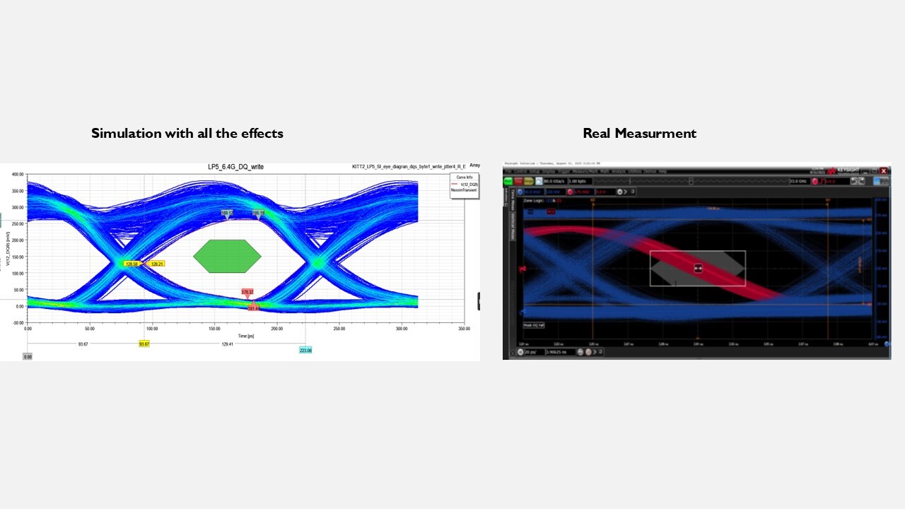
Infotainment systems in vehicles are undergoing a significant transformation, driven by extensive digitalization and increasingly complex technologies. The high design requirements for high-speed signal interfaces on infotainment PCBs are difficult to meet with traditional validation processes—especially under growing time pressure. That’s why simulation during development plays a central role at Harman Becker Automotive Systems. Signal integrity is crucial for complex PCB designs, and the biggest challenge lies in replicating real-world conditions as accurately as possible in the simulation.
The rapid evolution of automotive systems, especially with the integration of advanced infotainment, ADAS (Advanced Driver Assistance Systems), and autonomous driving features, is significantly increasing system complexity. This is driven by the need for higher data throughput, real-time processing, and seamless integration of multiple high-speed signals (such as PCIe Gen5, UFS Gen4. LPDDR5x, DP, USB, LVDS, and Ethernet) within constrained physical spaces. Additionally, the push towards electrification and the integration of numerous sensors and modules further complicate the system architecture.
What Are the Challenges?
- Signal Integrity (SI) in High-Speed Data Lines: Ensuring clean, reliable signals over high-speed interfaces in a noisy automotive environment is challenging. Factors like crosstalk, EMI, and impedance mismatches can degrade signal quality.
- Electromagnetic Compatibility (EMC): As more electronic components are packed into vehicles, managing EMI and ensuring compliance with standards becomes increasingly difficult.
- Physical Constraints: Limited space and the need for robust, vibration-resistant connections make PCB layout and component placement critical.
- Power Integrity: Managing power delivery to sensitive high-speed components while minimizing noise and voltage fluctuations.
- Thermal Management: High data rates and dense component placement generate heat, which can affect signal performance and hardware reliability.
Business Case: Lower Costs, Fewer Iterations, Happier Customers
By using powerful simulation software such as Ansys HFSS 3D Layout and Ansys SIwave, Harman is able to make well-informed design decisions early in the development phase. Crucially, simulation at Harman is not just a technical aid — it’s a strategic lever:
- Significantly reduce the number of physical prototypes
- Shorten time-to-market
- Improve product quality
- Increase customer satisfaction
Reducing the prototype phase can save approximately 6–9 months in time-to-market!

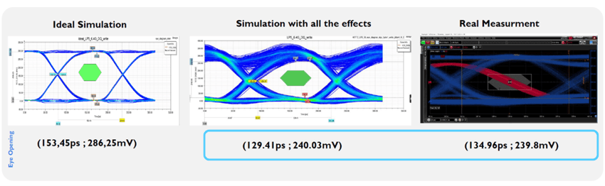
Comparison of simulation and measurement in eye diagrams for quantitative assessment of signal quality in high-speed data channels. | © Harman Becker Automotive Systems
Tailored Simulation Tools for Different Design Challenges
For low-complexity circuits and lower-speed interface designs, Harman engineers use Ansys SIwave to extract S-parameters, check impedance, and calculate trace lengths. Ansys SIwave is also used for power integrity simulations (DC and AC), and to simulate near and far-field effects for EMC.
For high-complexity circuits with high-speed interfaces, Ansys HFSS 3D Layout is employed to extract S-parameters with greater accuracy, leveraging cluster computing. When working with multiple PCBs, Ansys HFSS 3D Layout enables the combination of boards, including solder ball characteristics, to extract a unified set of S-parameters. These are then imported into Ansys Electronic Desktop, where component models are added to simulate TDR, eye diagrams, skew, insertion loss, return loss, crosstalk, and other parameters.
Tools and Technologies
- Ansys SIwave, Ansys HFSS, and Ansys HFSS Regions: Combination of 2.5D and 3D field solvers depending on complexity.
- Cluster Computing: Required for Ansys HFSS-based S-parameter extraction — implemented with support from CADFEM.
- Design Optimization: Example: Improved impedance by adjusting BGA solder ball diameters (from 51 to 69 Ohms).
Structured Process: Global Collaboration and Expertise Allocation
Harman follows a clearly defined simulation process. First, simulation goals are established in close coordination between stakeholders and simulation engineers. Then, relevant documents such as datasheets, models, and requirements are collected and reviewed. Depending on complexity and time constraints, different tools are selected for setup and analysis. Due to the high volume of tasks, responsibilities are distributed based on priorities and individual expertise. After final validation and documentation, the results serve as a decision-making basis for project management and development teams.
Details, Tips and Tricks
Learn more about "How to Simulate Close to Reality" and download the presentation by Dr. Maha Koraichi (Hardware Engineer, Engineering/R&D, Connected Car Division, Harman Becker Automotive Systems GmbH).
Get the presentation now
From Ideal to Reality: Challenges in High-Speed Design
The primary goal is to simulate as close to reality as possible. Instead of idealized setups, real-world effects such as power noise, jitter, PCB roughness, and etching processes are considered. This enables early identification and resolution of potential weaknesses — including worst-case analyses. Simulation allows every potential issue that could affect a system to be defined, identified, and resolved. By analyzing different scenarios, developers can test various ideas and technologies to stay ahead of global competitors.
Simulation Strategy
- Ideal Simulation: Starting point with simplified assumptions.
- Power-Aware Simulation: Integration of the Power Delivery Network (PDN) to account for feedback, simultaneous switching, and non-ideal return paths.
- Jitter Modeling: Inclusion of random, periodic, and deterministic jitter for realistic signal evaluation.
- Roughness & Etching Processes: Consideration of PCB manufacturing effects (e.g., Huray model) to improve TDR accuracy.
- Passive Components with S-Parameters: Realistic modeling of capacitors and inductors instead of idealized equivalent circuits.
Simulation Meets Reality: 90% Accuracy in Validation
After prototype completion, measurements are taken to determine key parameters and compare them with simulation results. The outcome: over 90% correlation (with result deviations of only 10%) — a testament to the high precision of the simulations. After each comparison, the simulation setup is reviewed for further improvement. This high level of accuracy builds trust with Harman’s customers and enables early, well-founded decisions throughout the development process.
Watch the interview with Dr. Maha Koraichi (Hardware Engineer, Engineering/R&D, Connected Car Division, Harman Becker Automotive Systems GmbH):
About Harman Becker Automotive Systems
Harman is a global leader in connected car technology, lifestyle audio innovations, professional audio and lighting solutions, and digital transformation. Our Automotive products are conceptualized by getting inside the minds of drivers and passengers alike to deliver the great experiences they love. Harman is driving a whole new world of possibilities through the expertise of our Automotive and Sound Engineers. It is delivering ‘ready’ products faster, while still upholding rigorous automotive standards. The result is new creative products at superior automotive grade.
FAQs
-
Why is realistic simulation essential for high-speed electronics design?
As data rates increase, even minor issues such as signal reflections, crosstalk, and electromagnetic interference can lead to performance degradation or data errors. Realistic simulation enables engineers to predict signal behavior in complex environments and address potential issues early in the design process. This reduces costly revisions and ensures reliable operation — resulting in robust, high-quality products that meet the demands of modern applications.
-
How do expanded simulation models improve accuracy in electronics development?
By including factors like power variations, timing uncertainties (jitter), and manufacturing tolerances, simulations become more representative of real-world conditions. This comprehensive modeling helps identify potential failures or bottlenecks early, reducing the risk of late-stage revisions and improving overall reliability.
-
What infrastructure and expertise are needed for effective electronics simulation?
A well-integrated simulation environment — supported by high-performance computing and detailed component models — enables faster and more accurate design cycles. These investments translate directly into competitive advantages in terms of speed, quality, and cost-efficiency.
-
Why is cross-functional collaboration important in simulation-driven electronics development?
Harman’s simulation strategy involves close cooperation between internal experts, layout engineers, CADFEM consultants, and Ansys specialists — especially during early design phases and iterations. This collaborative approach ensures that signal and power integrity challenges are addressed proactively, and new ideas for performance improvement are continuously explored.
Training on the Topic
-
RF Simulation with Ansys HFSS
In this course you will learn how to perform radio frequency 3D-Electomagnetic simulation with Ansys HFSS. This training is offered as a 2-day course or alternatively as a self-paced eLearning course.
-
Analyzing and improving EMC with simulation & measurement
In this training, you will learn how to effectively use simulation and testing in combination to get your electric device certified. This training is offered as a 3-day course.
-
EMC Analysis with Ansys EMC Plus: PCB, cables & housings
Learn to simulate complex EMC effects like radiation, shielding, coupling, and crosstalk using Ansys EMC Plus – in a fully digital workflow. This training is offered as a 2-day course.
-
Evaluate signal and power integrity of PCB designs with Ansys SIwave
In this training you will learn how to use simulation to accelerate and optimize the development process of PCBs. This training is offered as a 2-day course.