Beyond the 800G Optical Transceiver: Simulation-Driven Innovation for Next-Gen Networks

As optical transceivers push beyond 800G, engineers face mounting challenges in performance, integration, and scalability. In this interview with Dr. Despoina Petousi (Advanced Technology Senior Engineer, Adtran Networks SE) we will explore the key hurdles, the evolving role of silicon photonics, and how simulation – especially within the ANSYS CADFEM ecosystem – empowers innovation and system-level optimization.

Schalter sind standardisierte Serienprodukte. Das beschriebene Projekt wurde am Schaltwerk des Modells 506U durchgeführt | © JUNG  

Despoina, what are the key challenges for going beyond 800G in optical transceivers?

As we move beyond 800G in optical communication systems, the demands on transceiver performance are becoming more and more challenging to meet. The main drivers – AI applications, high-performance computing, and cloud infrastructure – are pushing bandwidth requirements to their physical limits. This means that devices need to support extremely high data rates while remaining power-efficient and compact.

One of the key challenges is that we no longer only need fast modulators – we need them to operate reliably in smaller footprints, with lower power consumption, and often in complex, co-integrated systems. At these speeds, even the smallest component – like a coupler or waveguide – must be highly optimized. You’re not just designing a device for performance anymore; you’re designing it for performance and system-level integration, yield, thermal stability, and fabrication robustness.

This leads to a shift in design thinking: instead of optimizing individual devices, we must now think in terms of complete ecosystems – integrating RF, photonics, electronics, and packaging in one tightly coupled design flow.

What Is an 800G Optical Transceiver and Why Does It Matter?

Optical transceivers are key components in modern data communication networks. They convert electrical signals into optical signals and vice versa to transmit data over fiber optic cables. These devices are used in data centers, telecommunications networks, and high-performance computing. The new generation of 800G (800 gigabits per second) transceivers is essential to meet the growing bandwidth demands driven by AI, cloud computing, and streaming. They enable faster, more energy-efficient data transmission in a compact form factor – making them a cornerstone of future digital infrastructure.

In your presentation you address various approaches to transceivers. Can you share your thoughts on this?

Yes, in my presentation I discussed different paths forward. The truth is, there is no one-size-fits-all solution for next-generation transceivers. While silicon photonics is still a very powerful platform – especially up to 800G – we do need to acknowledge that beyond this point, new materials will likely become necessary. For instance, when optimizing silicon modulators, we observe a typical trade-off: improving bandwidth often increases optical loss. This is due to the plasma dispersion effect in silicon, which inherently introduces loss through free carriers. 

That’s why new materials like lithium niobate become attractive for ultra-high-speed applications – they offer high bandwidth and low loss. That said, I believe the future of transceivers lies in hybrid systems: integrating novel materials like lithium niobate onto silicon, or co-packaging different functionalities. Silicon will remain essential – not just for the photonic core, but because of its compatibility with CMOS electronics. This enables monolithic integration of drivers and modulators, improving footprint and energy efficiency. So, instead of choosing one technology, we should look at how different technologies can complement each other.

Teaser_Blog_ADTRAN_Petusi

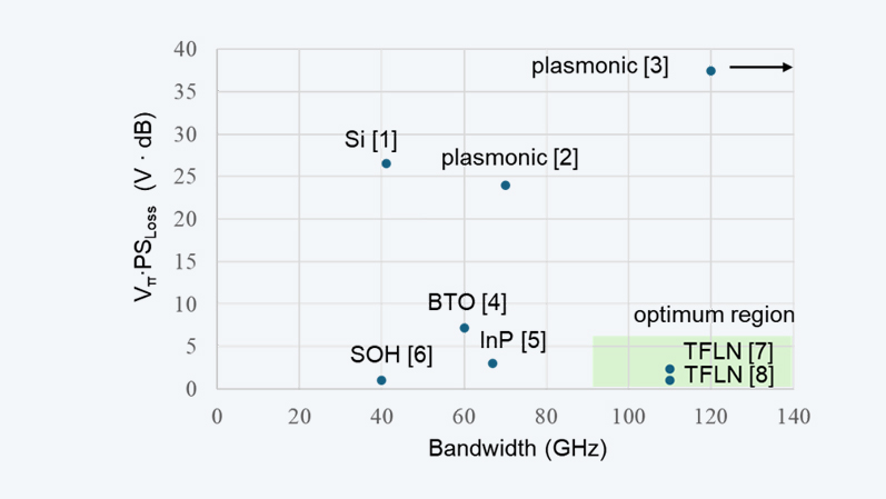
Modulator Material Technologies: Thin film lithium niobate (TFLN) MZMs show optimized performance | © Adtran

What are really the advantages of silicon photonics on the development of transceivers? 

Silicon photonics brings several key advantages to transceiver development, especially from a system and manufacturing perspective. First, it leverages the existing semiconductor infrastructure. Silicon foundries are mature, cost-effective, and offer high yield. This allows us to fabricate large-scale photonic integrated circuits on 300-mm wafers, which is extremely valuable for scaling production and reducing cost per unit.

Second, silicon photonics enables high integration density due to the high index contrast in the platform. This allows for very compact devices and complex routing within a small footprint, which is critical for co-packaging and next-gen modules.

Third – and perhaps most importantly – silicon photonics enables seamless integration with CMOS electronics. This means you can monolithically integrate modulators, photodetectors, amplifiers, and drivers onto the same chip. This drastically improves system performance by minimizing interconnect losses and latency, and it simplifies packaging, which is often a major bottleneck in high-speed systems.

Presentation: Simulation of Si Photonic Transmitters

Discover how simulation tools like Ansys Lumerical and Ansys HFSS can help you optimize your modulator designs for next-generation 800G transceivers.

Get the presentation now
Simulation of Si Photonic Transmitters

How important was it to use simulation tools in order to make decisions such as whether you prefer a certain setup or a certain solution for the transceiver?

Simulation is absolutely essential in our work. Transceivers are highly complex systems, and every component – whether a modulator, coupler, or photodetector – must be optimized for the application. We cannot rely on black-box models from a foundry if we want to push the limits of performance. In our group, Adtran simulates every component from scratch: starting with waveguide geometries, doping profiles, electro-optic responses, all the way to RF characteristics and thermal behavior. 

For example, in the modulator design process, Adtran uses tools like Ansys Lumerical and Ansys HFSS to simulate both optical and RF performance. This allows us to evaluate figures of merit like insertion loss, bandwidth, efficiency, and even thermal sensitivity before we ever go to fabrication. Another important point is yield. Even with the best designs, there are always discrepancies between simulations and actual measurements due to fabrication tolerances.

Having strong simulation models allows us to understand these discrepancies and build robust devices – ones that still perform well even when small imperfections occur. In short, simulation empowers us to design better, faster, and more reliably. It reduces risk, improves time-to-market, and enables smarter decisions throughout the entire development cycle.

With the CADFEM-Ansys ecosystem, we’re not just simulating components – we’re designing complete 800G systems. Cross-domain, precise, and scalable. Simulation isn’t just a tool – it’s the key to innovation.
Dr. Despoina Petousi
Advanced Technology Senior Engineer, Adtran Networks SE

What are the Roles of Ansys and CADFEM in Transceiver System Design?

The Ansys CADFEM ecosystem adds tremendous value because it provides a unified environment where different domains – photonics, RF, electronics, thermal, and packaging – can be co-designed and co-optimized. This is exactly what we need in a field where cross-disciplinary integration is no longer optional. For example, a change in the RF layout can affect the bandwidth of the modulator, which in turn can shift the thermal distribution across the package.

With Ansys, we’re able to bring all these aspects together – photonic simulation, electrical modeling, thermal analysis – and evaluate the full system in one place. This saves time, improves accuracy, and enhances collaboration between teams. Additionally, tools like Lumerical INTERCONNECT allow us to build full transceiver models – including signal modulation formats like 16-QAM – and evaluate system-level performance before tape-out.

This makes the development process much more predictable and gives us confidence that we are designing towards a functional, scalable product. To sum it up: the Ansys CADFEM ecosystem enables us not just to simulate devices, but to design complete systems. And in today’s world of complex, high-speed, integrated photonic platforms, that’s exactly what we need.

Watch now the full interview with Dr. Despoina Petousi:

About Adtran Networks SE

Adtran is a pioneer in open, disaggregated solutions with a shared vision for the future of fiber networking. We offer a comprehensive portfolio for providing homes, businesses and 5G infrastructure with scalable, secure and assured fiber connectivity, paired with cloud-managed Wi-Fi connectivity and SaaS applications.

 FAQs

Author

Klaus Kuboth

CADFEM Germany GmbH

+49 (0)8092 7005-279
kkuboth@cadfem.de