EMC Testing: Develop Reliable Electronics in 7 Steps
Klaus Kuboth
27.11.2025
A practical guide to robust, EMC-safe electronics
Strong electromagnetic compatibility (EMC) is essential for reliable electronics. Only then can systems operate smoothly—without interfering with other devices or being affected themselves. However, compact designs and high data rates make this increasingly challenging. In this article you'll explore how to create a strong foundation with a 7-step workflow for targeted EMC simulation.
Why a strategic approach to EMC simulation matters
Achieving reliable EMC isn’t about pushing a button at the project’s end. It demands a strategic, iterative approach, embedded into every step of development. That starts with the PCB, where high-frequency currents and critical interactions most often originate. The following 7 step process helps your team catch hidden EMC risks early, optimize for compliance, and move confidently toward a robust, interference-resistant product.
Step 1: Validate ECAD data for robust PCB design
The quality of your simulation is only as good as your input data. Overlooking routing details or a subtle layout artifact in your PCB is an easy way to let hidden EMC issues go unnoticed until late-stage testing – when fixes are far more costly. A precise digital model ensures that your analysis captures all the “real world” pitfalls.
In Ansys SIwave, import your ECAD files to build a high-fidelity representation of your board. SIwave’s 2.5D solvers efficiently analyze signal and power integrity (SI/PI), highlighting early concerns such as impedance mismatches, voltage drops, or ground bounce areas. Quickly visualize where your design might violate EMC basics and set your downstream analysis up for success.
Whitepaper: Designing Reliable Electronic Components
Learn how early EMC simulation enhances reliability and safety.
Read the Whitepaper on EMC Simulation now
Step 2: Identify resonances and coupling effects
With the early “hot spots” identified, dig deeper into why these problems occur. Is there an unwanted resonance? Is there excessive coupling between parallel traces? Are signal reflections tied to poor impedance matching? Pinpointing these specific causes ensures fixes are targeted and effective.
Leverage Ansys Slwave’s frequency sweeps and S-parameter analysis to identify resonances, analyze coupling paths, and visualize field distributions. The tool’s diagnostic views help you locate which physical structures – planes, traces, via groups – are causing the issue.
Step 3: Optimize layout and improve decoupling strategies
EMC is not an afterthought; it’s engineered into the design, trace by trace. The sooner you optimize layout, placement, and decoupling in response to identified EMC risks, the more robust and cost-effective your product will be. Fixing the identified root causes at the source might include rerouting critical traces, relocating components, optimizing stack-ups, removing split planes, or strengthening decoupling strategies.
Make layout adjustments in your ECAD tool, then update the Ansys Slwave model for a new round of analysis. “What-if” iterations help you see the real impact of routing changes, stack-up revisions, or added ground/decoupling, reducing the trial-and-error cycle.
Step 4: Ensure signal integrity through circuit analysis
Real-world EMC issues often crop up at the intersection of layout and circuit dynamics, including the influence of both intentional design and parasitic effects. Merging board-level simulation with full circuit analysis provides a true system perspective.
Export the transmission characteristics of key traces from Anys Slwave. Bring this data into Ansys AEDT Circuit for a system-level simulation. Here, you can identify precise signal waveforms, which serve as a crucial input source for subsequent analyses of interference fields. This helps you gain an understanding of dynamic circuit behavior as well as the effects of parasitics on system performance.

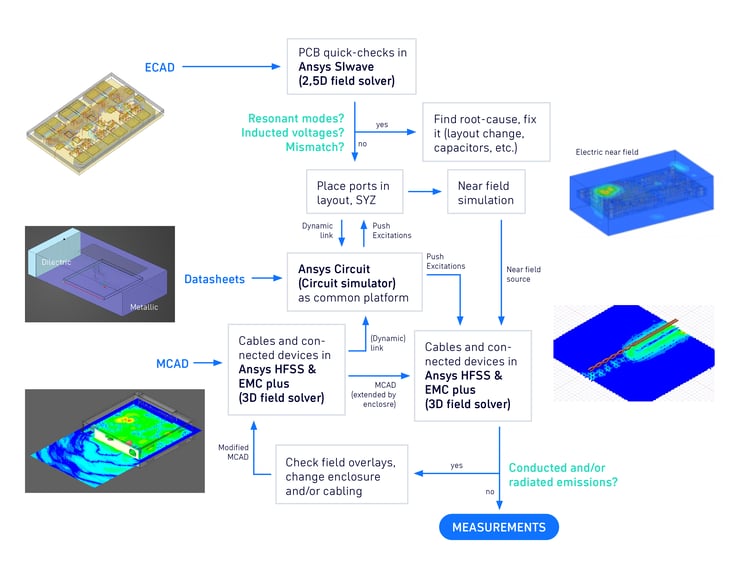
EMC Workflow in 7 Steps © CADFEM Germany GmbH
Step 5: Near-field and far-field analysis for interference hotspots
After understanding your circuit’s behavior, evaluate how much electromagnetic energy is leaking out. Mapping these near and far fields allows you to analyze its shape as it leaves your board. Identify likely trouble areas needing shielding, improved ground, or layout changes.
Transfer the signal waveforms determined in Ansys AEDT Circuit back to Ansys Slwave to calculate electromagnetic fields near and above the PCB, as well as those radiated further out. Use the data to visualize field strength and direction, identifying hotspots that could cause compliance headaches or unexpected interference.
Step 6: Full-wave simulation for complete system behavior
True EMC depends on everything – the board, the cables, the connectors, and the enclosure – acting together. That’s where you focus next: analyzing the device’s behavior in its operational environment. That is, not just the PCB, but the complete system. This comprehensive simulation identifies sources of radiated EMC problems and prepares for real-world interactions.
Take the near-fields calculated by Ansys SIwave and use them as excitation sources in a full 3D electromagnetic simulation with Ansys HFSS or Ansys EMC Plus. These tools model your system behavior under regulatory test conditions, revealing coupling, field penetration, and where shields and placement changes will have the greatest impact.
Step 7: Physical measurements and compliance validation
If you need to validate your simulation by mirroring the real test setup – now is the time. Aligning digital predictions with physical compliance measurements confirms that your workflow is on target, and pinpoints where refinement is still needed.
Integrate your test accessories and physical setup into your Ansys 3D model. When lab data becomes available, overlay those results with your simulations. Calibrate material properties or tweak model assumptions if needed. This way, the effort for building the measurement setup pays off, as you can use this loop to improve simulation accuracy for future projects.

Electronic Circuit Board Components | © Adobe Stock/CADFEM Germany GmbH
Conclusion: EMC simulation as the key to product reliability
Mastering EMC simulation isn’t just about technology. It’s about embedding reliability and compliance into your entire engineering process, from the PCB upwards. By following this structured workflow and leveraging the right tools at each stage, you can turn complex EMC challenges into opportunities for smarter, faster, and more predictable product development. As electronics continue to miniaturize and design cycles accelerate, this proactive approach gives you the competitive edge to innovate with confidence.